![]() Atomic Force Microscopy (MECA AFM)
Atomic Force Microscopy (MECA AFM)
| |
|
|
Previous Next |
|
See also See also
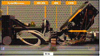
The Atomic Force Microscope (AFM) is part of the MECA Microscopy Station, which comprises a Sample Wheel and Translation Stage (SWTS), an optical microscope (OM), and the AFM. As shown in Figure 1, the MECA AFM is located between the OM and the SWTS inside the darkened MECA enclosure on the spacecraft deck. It scans a small region (from 1-65 µm square) on any of 69 substrates, each 3-mm in diameter, positioned along the rim of the SWTS. The chief scientific objectives of the AFM are to analyze small dust and soil particles in terms of their size, size distribution, shape, and texture. The AFM is particularly well suited to analyze particles carried by the wind, which are believed to be in the size range 1-3 µm.
Prior to AFM scanning, OM images are acquired to document the substrates and provide context for the AFM scans. OM data is described in the Phoenix camera SIS, along with the RAC and SSI, and is outside the scope of this document. The reader is also referred to that document for more detailed description of the SWTS and its substrates.
The AFM is contributed by a Swiss-led consortium spearheaded by the University of Neuchatel. Run by a dedicated microcontroller, the AFM uses one of an array of eight micromachined cantilevers with sharp tips to obtain topographs (sometimes called "scans" or "images") of up to a 65×65-µm area of the sample. Within this constraint the scan can be of any size, dimension, or orientation, but the AFM can only address a narrow horizontal stripe of each substrate. Since the sample wheel can be rotated (but not elevated) prior to initiation of scanning, the AFM can access a thin band approximately 1/3 of the way up from the bottom of the corresponding OM image. Note that the x and y axes of the MECA AFM image are rotated by +45 degrees relative to the OM images (figure 2).
Figure 1. Left: The SWTS translates in and out to collect samples, remove excess material, focus, and approach the AFM. It rotates to select any of 69 substrates. Right: The sampling chute, viewed from the top with 6 substrates exposed
The 69 substrates on the SWTS are divided into ten sets of six (a weak and a strong magnet, two "microbuckets", a textured substrate, and a sticky silicone pad) and nine utility or calibration targets. Using the SWTS, these can be coated with a thin layer of dust or soil, and then rotated to the vertical scanning position where they can be imaged by the optical microscope. Of the six substrates in each set, two are specifically designed for AFM use in that they resist the tendency for particles to become dislodged and to adhere to the AFM tip. Such particle adhesion can degrade the scans in question and the quality of the tip in general. One of these substrates is a uniform piece of silicone that remains pliant under martian conditions. The second is a custom micro-machined silicon substrate with pits and posts that hold particles of an appropriate scale for AFM scanning. Two of the remaining four substrates are magnets that may, under certain circumstances, be appropriate for AFM scanning. The final two substrates are deep "buckets" that would not normally be accessible to the AFM.
To operate the microscopy station, soil samples are deposited by the RA (or dust from the air) onto a segment of the SWTS ring that has been extended such that exactly one set of 6 substrates protrudes from a horizontal slot in the MECA enclosure. Excess material is removed by passing the substrates under a blade positioned 0.2 mm above the surface, after which the samples are rotated for imaging by the OM and AFM. The exposed substrates are then rotated from their horizontal load positions into their vertical imaging positions. The SWTS is also used for focusing and AFM coarse positioning.
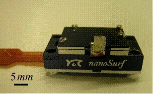
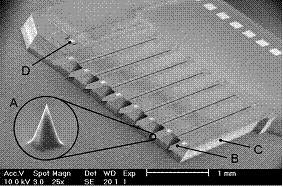
MECA's AFM comprises three major components, a microfabricated probe-chip, an electro-magnetic scanner-actuator and single board control electronics. The probe-chip features 8 cantilevers, numbered 0-7. The chip is mounted with two orthogonal tilt angles of 10 degrees relative to the sample to ensure that only one tip contacts the sample at a time. In case of contamination or malfunction of this front-most tip, the defective cantilever and its support beam can be cleaved off by a special tool on the sample wheel, after which the next one in the array becomes active. The force constant of the levers varies between 9 and 13 N/m.
Each of the 8 MECA cantilevers features an integrated piezo-electric stress sensor, which is used to measure its pure deflection (static mode) or its vibration amplitude, frequency and phase (dynamic mode). In static mode the deflection signal is proportional to the force, while in dynamic mode the shift of the resonance frequency is a measure of the force gradient. Dynamic mode minimizes the interactions between tip and surface and is less likely to result in particles being moved around or dislodged during the scan. In either mode, these signals are used to regulate the distance between the tip and the sample in the z-direction by means of a proportional-integral feedback loop.
The z-axis servo signal represents the sample topography as the tip is rastered across the surface in the x (fast) and y (slow) directions. (Though the resulting topograph is sometimes referred to as an image, it bears little resemblance to an optical image until it is transformed and processed.) Imperfect feedback or an out-of-range condition can result in residual bending of the cantilever in static mode, or a phase shift of the oscillation in dynamic mode. This error signal may optionally be recorded in a second data channel. Since each line in the raster scan begins at the same point on the x-axis, both primary and error signals may be recorded either on the forward or the backward legs of the scan (or, typically, both). Thus a single raster scan can produce up to four arrays of data: Forward (signal), forward (error), backward (signal), and backward (error), each of which can be displayed in image format.
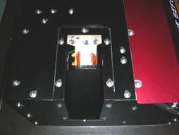
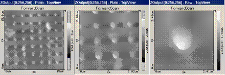
Figure 2. Upper Left: The AFM scanner viewed from the perspective of the sample. Upper right: The scanner positioned under the nose of the OM and in front of the SWTS. Lower left: The AFM chip. (A) is a close-up of one of the silicone tips, (B) points is one of 8 cantilevers mounted on a cleavable support-beam (C). D) is a reference piezoresistor used for temperature compensation. Lower Right: topographs of pincushion array with increasing magnification.
Source: MECA Non Imaging EDR SIS
|